
CDM
EquipmentCharged Device Model
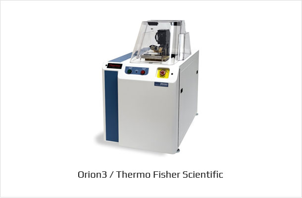
Orion3 / Thermo Fisher Scientific
Introduction
This test models the phenomenon in which semiconductors and electronic parts become charged due to friction and contact, and rapid discharge occurs when the charged parts contact a conductor. ESD does not incur any defects if it can be implemented in a only No Charge or only No Discharge environment. However, since it is impossible to remove the source of static electricity, the level of tolerance of ICs and electronic components must be assessed.
Application
Semiconductor(Memory, System IC), DIscrete IC, Passive Component Level ESD(CDM) Test, Board-level CBM (Charged Board Model) Test
The Equipment
HBM & MM Equipment
-
- Equipment
-
Max. Voltage Level : 2000V
Max. Test Area : 10.16 x 10.16cm
CDM Method : Field Induced Charge, Direct Charge
Monitoring and Controlling N2 flow
Reporting humidity & temperature levels
Technical Use Case
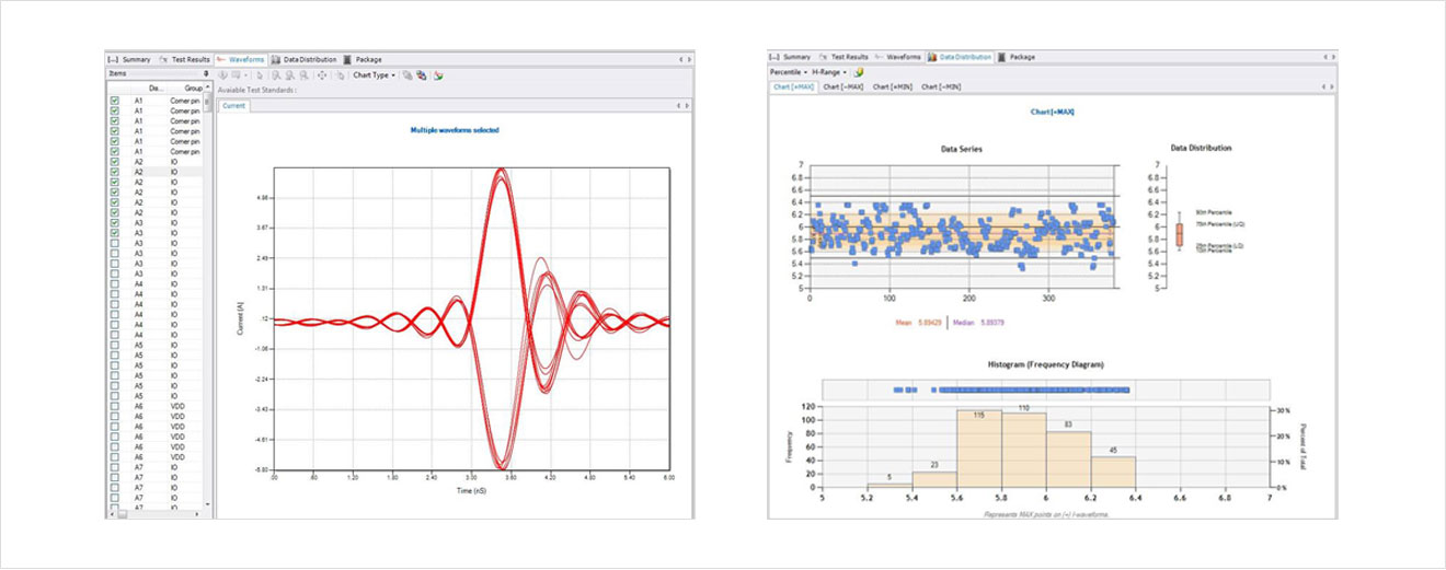
Automated Waveform Measurement & Analysis
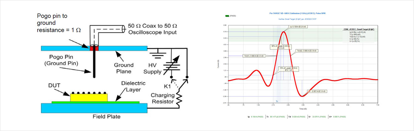
Simulator Circuit & Stand Waveform
Related Standards
Items |
Consumer / Industrial |
Automotive |
|---|---|---|
CDM |
JS-002-2018 |
• AEC-Q100-011 • AEC-Q101-005 |
Contact Point
Person in chargeSenior Engineer
- • TEL.
- +82-31-546-7549
- • E-mail.
- dongsung.kim@qrtkr.com