
FIB Circuit edit
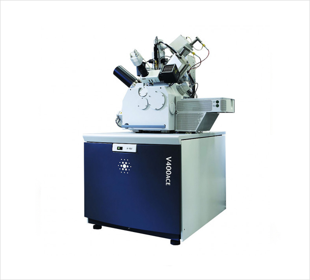
EquipmentSingle Beam Focused Ion Beam
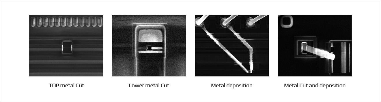
Single Beam FIB is used to modify the circuit of the semiconductor chip by cutting or connecting the metal wiring within the semiconductor chip.
Introduction
Focused ion beam (FIB) can be shot with an ion beam to etch fine areas, and can be used to deposition metallic materials such as tungsten(W), platinum(Pt) or non-metallic materials such as TMCTS into desired shapes. Using these characteristics of the FIB, circuits of the semiconductor chip can be edited. If a circuit design anomaly is detected in the process, the circuit must be physically modified. In such a case, the FIB can modify the circuit and verify its electrical operating characteristics in a short time. The FIB's quick design verification allows it to be more time and cost effective than changing the mask.
Application
Al metal Circuit edit, Cu metal Circuit edit, Backside circuit edit, Probing pad
The Equipment
-
- Manufacturer / Model
ThermoFisher / V400 ACE
-
Feature
Description
Function
Circuit Modification (Cu, Al, Backside)
Column
Tomahawk, Ga liquid metal 1000 hour lifetime
Acceleration Voltage
0.5 kV - 30 kV
Image Resolution
4.5 nm
Beam Current
1.1 pA - 65 nA
Stage
5 axis all piezo motorized X, Y motion 100 mm
Nano Chemix Gas Delivery
𝑋𝑒𝐹2, TMCTS, 𝐻2𝑂, 𝑂2, W
End Point Detect
Simultaneous SE Specimen current auto scaled plots
Technical Use Case
Circuit edit
Probing Pad Manufacturing

Contact Point
Person in charge- • TEL.
- 031-546-7555
- • E-mail.
- sunghoo.park@qrtkr.com